Scaling laws of edge and bulk charge transport in twisted graphene interfaces
Distinguishing edge vs. bulk charge transport using nanomanipulation of twisted graphene interfaces, taken from Nat. Commun. 11, 4746 (2020).
The unusual electronic properties of edges in graphene-based systems originate from the pseudospinorial character of their electronic wavefunctions associated with their non-trivial topological structure. This is manifested by the appearance of pronounced zero-energy electronic states localized at the material zigzag edges that are expected to have a significant contribution to the interlayer transport in such systems. In this work, we utilize a unique experimental setup and electronic transport calculations to quantitatively distinguish between edge and bulk transport, showing that their relative contribution strongly depends on the angular stacking configuration and interlayer potential. Furthermore, we find that, despite of the strong localization of edge state around the circumference of the contact, edge transport in incommensurate interfaces can dominate up to contact diameters of the order of 2 mm even in the presence of edge disorder. The intricate interplay between edge and bulk transport, may have profound consequences on practical applications of nanoscale twisted graphene-based electronics.
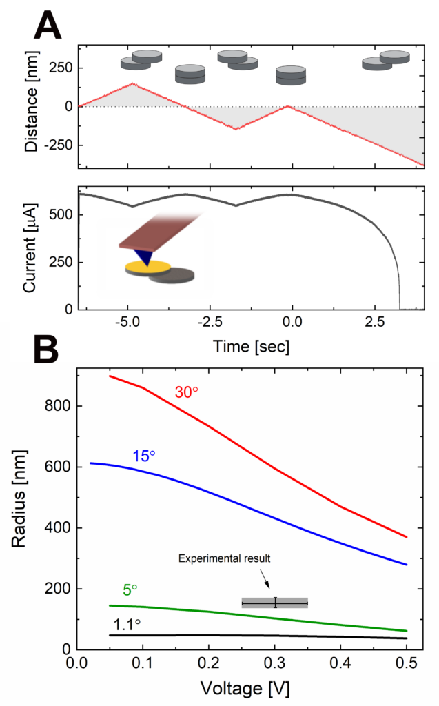
Electromechanical manipulation of layered materials

Nano-manipulation of metastable graphitic structures. Science, 2015, 348 (6235), 679-683
The weak interlayer binding in 2-dimensional layered materials such as graphite gives rise to intricate mechanical and electronic properties in particular if the atomic lattices at the interface are rotated with respect to one another. The lack of crystal symmetry leads to special correlations of the pz orbital interactions across the twisted interface, which gives rise to low friction behavior and anomalous electrical interlayer transport. This mechanism allows to design unique nanometer electromechanical devices (NEMS).
Charge transport in twisted graphene interfaces
Interlayer conductivity and coherent commensurate electronic states at the interface between misoriented graphene layers. Nature Nanotechnology, 2016, 11, 752-757.
Using our nano-manipulation technology we study the out-of-plane electrical conductivity of twisted graphene interfaces. The measurement reveals that the electrical transport across the interface is dominated by a phonon assisted channel. Most intriguingly, the conduction is significantly enhanced within a narrow angular range at “magic” angles of 21.8º and 38.2º providing the first experimental confirmation for the existence of a novel 2-dimensional interface state originating from the coherent coupling of electronic states in the twisted sheets due to the commensurate superlattice.
Nanoscale electronic characterization of low dimensional materials and devices
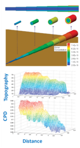
Dopants concentration distribution measurement of a single Si nanowire using Kelvin Force Probe Microscopy (KPFM). Nano letters, 10, 4 (2011).
We have developed an experimental method that allows to measure the active dopant distribution in individual silicon nanowires grown by the vapor−liquid−solid (VLS) method. Our method is based on successive surface etching of a portion of a contacted nanowire, followed by measurement of the potential difference between the etched and unetched areas using Kelvin probe force microscopy (KPFM). The radial dopant distribution is obtained by fitting the measured potentials with a three-dimensional solution of Poisson equation. We have found that the radial active dopant distribution decreases by almost 2 orders of magnitude from the wire surface to its core even when there is no indication for tapering. In addition, the dopant profile is consistent with a very large diffusion coefficient of D ∼ 1 × 10⁻¹⁹ m2 s−1.
Electronic contact analysis
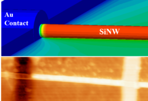
Surface potential measurement of a reversed biased Schottky contact made of n-type Si nanowire and gold metallic electrode. APL, 99 (2011).
Kelvin probe force microscopy is used to measure the surface potential of both doped and intrinsic Si nanowires Schottky junctions. The imaging of the Schottky junction together with 3D potential simulation and consideration of the convolution of the scanning tip enables us to determine the real potential. Analysis of the potential drop under different reversed bias conditions allows to extract dopants concentration, mid-gap traps and surface charge.
Friction in the superlubricity regime
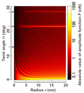
Scaling of the lateral sliding force as a function of both angular mismatch and contact radii. Phys. Rev. B, 2016, 94, 045401
The weak interlayer binding in two-dimensional layered materials such as graphite gives rise to distinguished low-friction properties if the atomic lattices at the interface are rotated with respect to one another. The lack of crystal symmetry leads to poorly understood correlations and cancelations of the interlayer atomic forces. Recently, we reported on a powerful tiling method based on the moiré superstructure which allows us to study the intricate interplay of the interlayer forces in a systematic manner.